- 您现在的位置:买卖IC网 > Sheet目录481 > MTP2P50E (ON Semiconductor)MOSFET P-CH 500V 2A TO-220AB
�� �
�
�MTP2P50E�
�12�
�Q� T�
�300�
�1000�
�V� DD� =� 250� V�
�10�
�8�
�Q� 1�
�Q� 2�
�V� GS�
�250�
�200�
�I� D� =� 2� A�
�V� GS� =� 10� V�
�T� J� =� 25� °� C�
�6�
�4�
�I� D� =� 2� A�
�T� J� =� 25� °� C�
�150�
�100�
�100�
�t� f�
�t� d(off)�
�2�
�0�
�0�
�2�
�4�
�Q� 3�
�6�
�8�
�10�
�12�
�14�
�V� DS�
�16�
�18�
�50�
�0�
�20�
�10�
�1�
�10�
�t� r�
�t� d(on)�
�100�
�Q� T� ,� TOTAL� CHARGE� (nC)�
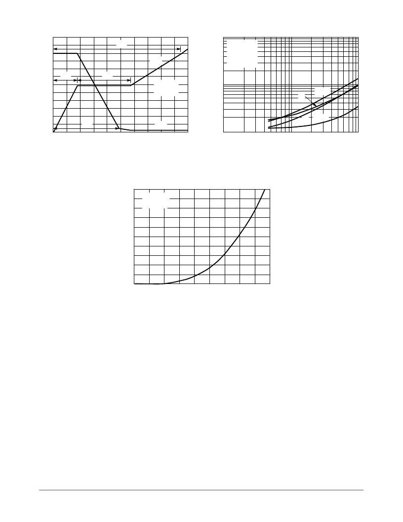
�Figure� 8.� Gate� ?� To� ?� Source� and� Drain� ?� To� ?� Source�
�Voltage� versus� Total� Charge�
�R� G� ,� GATE� RESISTANCE� (OHMS)�
�Figure� 9.� Resistive� Switching� Time�
�Variation� versus� Gate� Resistance�
�DRAIN� ?� TO� ?� SOURCE� DIODE� CHARACTERISTICS�
�2�
�1.6�
�1.2�
�0.8�
�0.4�
�0�
�V� GS� =� 0� V�
�T� J� =� 25� °� C�
�0.6�
�0.8�
�1�
�1.2�
�1.4�
�1.6�
�1.8�
�2�
�2.2�
�2.4�
�V� SD� ,� SOURCE-TO-DRAIN� VOLTAGE� (VOLTS)�
�Figure� 10.� Diode� Forward� Voltage� versus� Current�
�SAFE� OPERATING� AREA�
�The� Forward� Biased� Safe� Operating� Area� curves� define� the�
�maximum� simultaneous� drain� ?� to� ?� source� voltage� and� drain�
�current� that� a� transistor� can� handle� safely� when� it� is� forward�
�biased.� Curves� are� based� upon� maximum� peak� junction�
�temperature� and� a� case� temperature� (T� C� )� of� 25� °� C.� Peak�
�repetitive� pulsed� power� limits� are� determined� by� using� the�
�thermal� response� data� in� conjunction� with� the� procedures�
�discussed� in� AN569,� “Transient� Thermal� Resistance� ?� General�
�Data� and� Its� Use.”�
�Switching� between� the� off� ?� state� and� the� on� ?� state� may�
�traverse� any� load� line� provided� neither� rated� peak� current�
�(I� DM� )� nor� rated� voltage� (V� DSS� )� is� exceeded� and� the�
�transition� time� (t� r� ,t� f� )� do� not� exceed� 10� m� s.� In� addition� the� total�
�power� averaged� over� a� complete� switching� cycle� must� not�
�exceed� (T� J(MAX)� ?� T� C� )/(R� q� JC� ).�
�A� Power� MOSFET� designated� E� ?� FET� can� be� safely� used�
�reliable� operation,� the� stored� energy� from� circuit� inductance�
�dissipated� in� the� transistor� while� in� avalanche� must� be� less�
�than� the� rated� limit� and� adjusted� for� operating� conditions�
�differing� from� those� specified.� Although� industry� practice� is�
�to� rate� in� terms� of� energy,� avalanche� energy� capability� is� not�
�a� constant.� The� energy� rating� decreases� non� ?� linearly� with� an�
�increase� of� peak� current� in� avalanche� and� peak� junction�
�temperature.�
�Although� many� E� ?� FETs� can� withstand� the� stress� of�
�drain� ?� to� ?� source� avalanche� at� currents� up� to� rated� pulsed�
�current� (I� DM� ),� the� energy� rating� is� specified� at� rated�
�continuous� current� (I� D� ),� in� accordance� with� industry�
�custom.� The� energy� rating� must� be� derated� for� temperature�
�as� shown� in� the� accompanying� graph� (Figure� 12).� Maximum�
�energy� at� currents� below� rated� continuous� I� D� can� safely� be�
�assumed� to� equal� the� values� indicated.�
�in� switching� circuits� with� unclamped� inductive� loads.� For�
�http://onsemi.com�
�5�
�发布紧急采购,3分钟左右您将得到回复。
相关PDF资料
MTP3055VL
MOSFET N-CH 60V 12A TO-220AB
MTP3055VL
MOSFET N-CH 60V 12A TO-220
MTP3055V
MOSFET N-CH 60V 12A TO-220AB
MTP36N06V
MOSFET N-CH 60V 32A TO-220AB
MTP50P03HDL
MOSFET P-CH 30V 50A TO-220AB
MTPD1346-010
PIN DIODE 1300NM FLAT 2.8MM TO46
MTPD1346-030
PIN DIODE 1300NM FLAT 2.8MM TO46
MTPD1346-100
PIN DIODE 1300NM FLAT 2.8MM TO46
相关代理商/技术参数
MTP2P50E_10
制造商:ONSEMI 制造商全称:ON Semiconductor 功能描述:Power MOSFET 2 Amps, 500 Volts
MTP2P50EG
功能描述:MOSFET 500V 2A P-Channel RoHS:否 制造商:STMicroelectronics 晶体管极性:N-Channel 汲极/源极击穿电压:650 V 闸/源击穿电压:25 V 漏极连续电流:130 A 电阻汲极/源极 RDS(导通):0.014 Ohms 配置:Single 最大工作温度: 安装风格:Through Hole 封装 / 箱体:Max247 封装:Tube
MTP2S-E10-C
功能描述:电缆束带 Multiple Tie Plate 2 Bund, M-S ties #10 RoHS:否 制造商:Phoenix Contact 产品:Cable Tie Mounts 类型:Adhesive 颜色:Black 材料:Acrylonitrile Butadiene Styrene (ABS) 长度:19 mm 宽度:19 mm 抗拉强度:
MTP2S-E10-C39
功能描述:电缆束带 Mutiple Tie Plate, 2 Bundle, M-S Ties, # RoHS:否 制造商:Phoenix Contact 产品:Cable Tie Mounts 类型:Adhesive 颜色:Black 材料:Acrylonitrile Butadiene Styrene (ABS) 长度:19 mm 宽度:19 mm 抗拉强度:
MTP2S-E6-C
功能描述:电缆束带 Mutiple Tie Plate, 2 Bundle, M-S Ties, # RoHS:否 制造商:Phoenix Contact 产品:Cable Tie Mounts 类型:Adhesive 颜色:Black 材料:Acrylonitrile Butadiene Styrene (ABS) 长度:19 mm 宽度:19 mm 抗拉强度:
MTP3
制造商:VISHAY 制造商全称:Vishay Siliconix 功能描述:Three Phase Bridge (Power Module) 45 A to 100 A
MTP30
制造商:NELLSEMI 制造商全称:Nell Semiconductor Co., Ltd 功能描述:Glass Passivated Three-Phase Bridge Rectifier, 30A
MTP3001N3
制造商:CYSTEKEC 制造商全称:Cystech Electonics Corp. 功能描述:P-CHANNEL ENHANCEMENT MODE POWER MOSFET